HomeAboutServicesCase Study — PCB HousingPortfolioContact Us

Precision ABS PCB Housing Case Study (±0.02mm Critical Tolerance)

High-precision ABS electronic enclosure developed for consistent PCB fitment and zero cosmetic defects across high-volume production.

Proven Results

±0.02mm Tolerance Achieved 100,000+ Parts Delivered Zero Dimensional Complaints

Material

ABS

Part Size

~37mm Profile

Tolerance

±0.02mm

Localized Thickness

0.30–0.35mm

Volume

100,000+

OverviewChallengeSolutionResultsTakeaways
Precision ABS PCB housing enclosure showing locating pins and thin wall sections
ABS electronic housing close-up showing cosmetic surface and PCB mounting features
Application

Project Overview

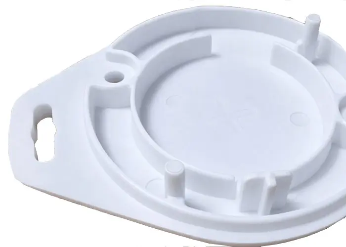
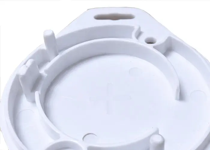
This project involved the development and production of a precision injection molded ABS electronic housing designed for secure PCB mounting. The component required high dimensional stability and tight tolerance control to ensure consistent PCB seating during assembly. The part was produced in high volumes over a sustained production cycle, with strict quality expectations for both functional and cosmetic performance.

The Problem

Engineering Challenge

The primary challenge was maintaining ±0.02mm positional accuracy in critical PCB locating zones. Even minor shrinkage variation or dimensional drift resulted in PCB misalignment, leading to assembly rejection risks.

Additionally, the part included localized thin-wall sections (~0.30–0.35mm), increasing the complexity of material flow and shrinkage control. The visible surfaces required zero gate marks, adding a cosmetic constraint alongside dimensional precision.

Specific Challenges

  • 37mm ABS housing with internal PCB location requirement
  • Critical locating pins (Ø ~1.7mm) requiring ±0.02mm positional accuracy
  • Localized thickness (~0.30–0.35mm) in critical areas
  • Zero visible gate mark requirement (cosmetic surface)
  • PCB seating failure if deviation exceeded 0.02mm
Our Approach

Engineering Solution & Process Control

DFM Validation

Dual-stage DFM validation to optimize part geometry and tooling approach. Identified critical areas requiring localized process control.

Gate Strategy

Core-side banana gating to eliminate visible gate marks on cosmetic surfaces while maintaining optimal material flow to critical geometry.

Shrinkage Control

Localized shrinkage control in thin-wall regions through optimized tool design and controlled cooling strategy for dimensional stability.

Cooling & Stabilization

Controlled cooling strategy to ensure dimensional stability and reduce warpage across the thin-wall geometry. Optimized cycle parameters for consistent repeatability.

Structured Validation

Structured T0 and T1 validation trials for dimensional verification before mass production release. Process parameters locked after qualification.

Results

Production Outcome

±0.02mm

Tolerance Achieved

100%

PCB Fitment Success

100K+

Parts Delivered

Zero

Dimensional Complaints

Insights

Key Engineering Takeaways

Tight tolerance injection molding requires localized process control, not just global tool accuracy. Critical dimensions must be managed at the feature level.

Thin-wall geometries significantly influence shrinkage behavior and must be managed during DFM — not corrected after tooling.

Gate location selection directly impacts both cosmetic quality and dimensional consistency. Core-side gating solves both simultaneously.

Structured validation (T0/T1) is critical for achieving repeatability in mass production. Process parameters must be locked before volume release.

Have a Similar Precision Requirement?

If your application requires tight tolerance control, high repeatability, or complex geometry, our team can support your project from DFM through production.
Share your drawing / requirement for review.

Discuss Your Requirement →View All Services